GF Securities published a research report that semiconductors are highly capital-intensive and highly technology-intensive industries, and are a must for the world's major powers. As the largest consumer market of global semiconductors, China's semiconductor industry is imperative in terms of geographical support and national will, and the entire semiconductor industry chain is expected to continue to benefit. It is recommended to focus on SMIC (11.7, 0.62, 5.60%) (00981) and Hua Hong Semiconductor (14.98, 0.20, 1.35%) (01347) and ASM PACIFIC (the global semiconductor packaging and testing equipment manufacturer) with a certain scale. 124.6, -0.90, -0.72%) (00522). The global semiconductor industry is returning to the upward cycle. From the perspective of the industrial chain, the upstream of semiconductors mainly includes equipment and materials. The midstream IC production includes “design-manufacture-package-testâ€. The downstream applications are mainly concentrated in computers and consumers. Electronics, network communications, automotive electronics and other fields. 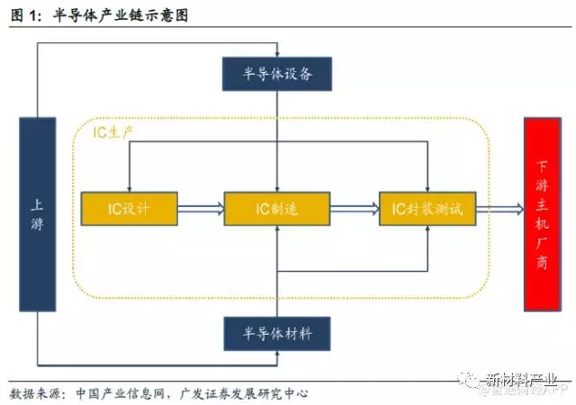 Semiconductor products are mainly divided into four parts: integrated circuit (IC), optoelectronics, discrete devices and sensors. According to WSTS statistics, in 2016, IC sales accounted for 82%, optoelectronics accounted for 9%, discrete devices accounted for 6%, and sensors accounted for 3%. Since IC sales accounted for more than 80% of semiconductor sales for many years, IC is generally referred to as a semiconductor in the market. In addition, integrated circuits are differentiated according to different functional uses, mainly including four categories: microprocessor (about 18%), memory (about 23%), logic chip (about 27%), and analog chip (about 14%). At present, the global IC industry has two business models: IDM (Integrated Device Manufacturer) mode and vertical division mode.
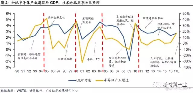
 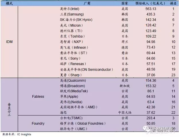 IDM refers to the business model that is completed by a company from design, manufacturing, packaging and testing to sales of its own IC products. Vertical division refers to the design, manufacture and packaging testing of ICs by professional IC designers (Fabless) and ICs. The business model undertaken by the manufacturer (Foundry) and the IC package tester (Package & Testing); At present, the IDM model still dominates the world. In 2016, global TOP20 manufacturers accounted for approximately 80% of global semiconductor sales. Among them, IDM manufacturers accounted for approximately 68% of the top 20, Fabless accounted for 18%, and Foundry accounted for 14%. The semiconductor industry is a cyclical industry, and its development has a high correlation with GDP, and the overall situation is positively correlated. In recent years, with the development of next-generation information technology in the fields of artificial intelligence, big data, Internet of Things, AR/VR, and wearable devices, the semiconductor industry has re-entered a new round of business cycle.
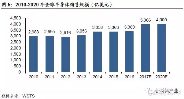
  According to the statistics of WSTS, the world's semiconductor trade statistics organization, the global semiconductor sales growth rate was 5.21% from 2003 to 2016, of which global semiconductor sales in 2016 reached 338.9 billion US dollars, an increase of 1.12%. WSTS expects global semiconductor sales to reach US$396.6 billion in 2017, a year-on-year growth rate of 17%. By 2020, the entire market is expected to reach a market size of US$400 billion.
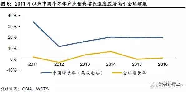
  In recent years, the demand for China's semiconductor market is strong, and the growth rate of the IC market is significantly higher than the global growth rate. According to WSTS statistics, China's semiconductor consumption in 2016 was 107.5 billion US dollars, accounting for 32% of the global total. It has surpassed the United States, Europe and Japan to become the world's largest market. At the same time, according to the China Semiconductor Industry Association (CSIA) statistics, China's IC sales in recent years maintained a double-digit growth rate, of which China's IC sales in 2016 increased by 20.1% year-on-year.
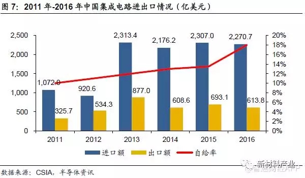
  But on the whole, the self-sufficiency rate of the domestic IC market is still at a low level, and the products are mainly imported from abroad.
  IC materials: domestic manufacturers step into the development of fast lane IC materials are mainly divided into IC manufacturing materials and IC packaging materials. The IC manufacturing materials mainly include silicon wafers and substrates, photomasks, photoresists, electronic gases, CMP materials, targets, etc.; IC packaging materials include laminated substrates, lead frames, bonding wires, molding compounds, and bottoms. Filler, liquid sealant, die bonding material, solder ball, etc. According to the International Semiconductor Industry Association (SEMI) report, the global IC manufacturing materials market was $24.7 billion in 2016 and the packaging materials market was $19.6 billion. Among them, among silicon manufacturing materials, silicon wafers account for the highest proportion of 32%, and silicon wafers and masks, electronic gases, CMP materials, and photoresists account for nearly 80% of the total, which is affecting the IC manufacturing process. The most important material. The wafer is the substrate for IC processing. From the development history of the wafer material, it can be roughly divided into three generations: the first generation is represented by germanium and silicon; the second generation is mainly gallium arsenide and indium phosphide; The third generation is gallium nitride, silicon carbide, and the like. At present, most wafers still use silicon as the main raw material. Judging from the global competition in silicon wafer materials, this market is dominated by Japanese manufacturers. According to the 2015 SEMI statistics, Japan's Shin-Etsu and SUMCO are leading manufacturers in the wafer production industry, and the two companies together account for about 50% of the market. According to the SEMI report, the size of the IC manufacturing materials market in China in 2016 was US$6.53 billion, which has become the fourth largest IC manufacturing materials market in the world, second only to Taiwan, South Korea and Japan. IC equipment: The trend of localization began to show that IC equipment is the upstream supporting equipment for IC production, and IC equipment is basically needed in IC design, manufacturing, packaging and testing. According to different functional uses, IC devices are generally classified into three categories: IC manufacturing equipment, IC packaging equipment, and IC testing equipment. Among them, IC manufacturing equipment has the largest variety and the largest proportion, such as lithography machine, etching equipment, film deposition and other core wafer processing equipment; IC packaging equipment mainly has bonding machine, laminating machine, etc.; IC test equipment mainly includes sorting machine , test machine, probe station, etc., suitable for the end of the IC design, manufacturing, packaging test.
 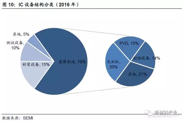 The IC equipment industry has high technical barriers, and currently European, American and Japanese manufacturers still occupy an absolute dominant position. Applied Materials, ASML, Tokyo Electronics, and Lam Research are the world's top four semiconductor device manufacturers with market shares of approximately 19%, 18%, 16%, and 15%, respectively. The rapid development of domestic downstream IC production links has driven the strong demand for domestic IC equipment market. According to SEMI's survey, China's semiconductor equipment market in 2016 was US$6.66 billion, up 31.8% year-on-year, and the fastest growth rate in the world, becoming the third largest semiconductor equipment market after Taiwan and South Korea. According to SEMI estimates, the demand for IC equipment by Chinese local companies will increase rapidly between 2018 and 2020. The estimated investment in IC equipment is US$10.8 billion, US$11 billion and US$17.2 billion, respectively. With the continuous improvement of market demand, domestic IC equipment manufacturers continue to increase research and development efforts. In the past two years, China has made breakthroughs in many key equipment fields. IC design: The domestic manufacturer's emerging IC design, Integrated Circuit Design, is the process of transforming the system, logic and performance design requirements into a specific physical layout. The IC design flow is divided into several steps: specification customization, hardware language description, simulation and simulation verification, logic synthesis, circuit simulation verification, circuit layout and surround, circuit detection, and mask production. According to IC Insights data, in the field of pure IC design (Fabless), the United States has the largest market share. In 2016, the total capacity of IC Fabless in the United States accounted for 62% of the global total. Qualcomm and Broadcom are leading companies in the IC Fabless industry, with combined revenues accounting for 51% of the top 10 revenues. Among them, Qualcomm's revenue in 2016 was 15.4 billion US dollars, and Broadcom's revenue was 15.3 billion US dollars.
 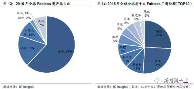 Benefiting from the demand in the domestic downstream mobile, communications and other fields, the competitiveness of domestic IC designers began to emerge. According to IC Insights statistics, there were only one mainland Chinese company in the TOP50 Fabless business in 2009. By 2016, the number of mainland Chinese enterprises has reached 11 and the combined market share has increased to 10%. Among them, Huawei HiSilicon and Spreadtrum have become among the top 10 Fabless in the world.
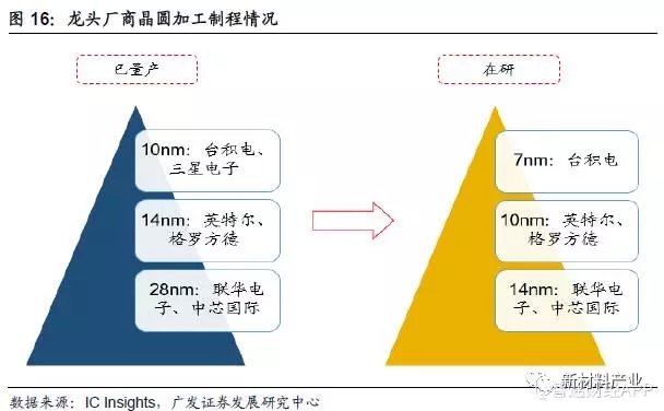
 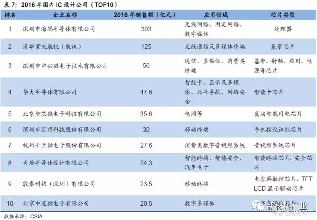 IC manufacturing: The policy support is the strongest, and domestic manufacturers are eager to catch up with IC manufacturing to complete the process of integrated circuit etching on the wafer. The IC manufacturing process includes surface grinding, cleaning, coating, multiple lithography, ion implantation, etching, heat treatment, decanting, polishing, cleaning, inspection, packaging and other processes. At present, international leading manufacturers have developed process technology to 10nm level. Leading manufacturers such as TSMC and Samsung have achieved mass production in 10nm process. Intel and Grofund expect to achieve mass production by the end of this year. In addition, TSMC is taking the lead in developing 7nm process technology.
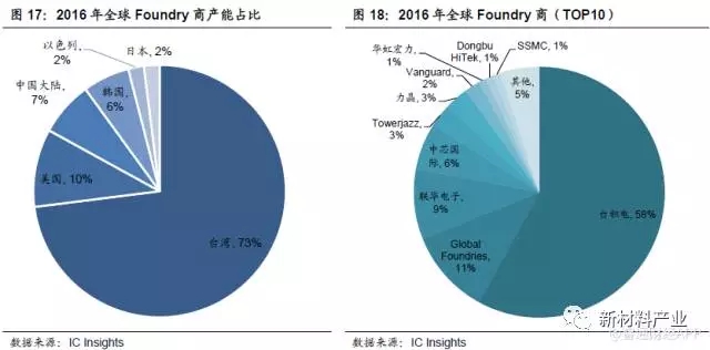
  According to IC Insights data, Taiwan has the largest market share in the field of pure IC manufacturing (Foundry). In 2016, the total production capacity of Foundry in Taiwan accounted for 73% of the global total. Among them, TSMC's revenue was US$28.57 billion, accounting for 58% of the global market share.
  IC manufacturing is a capital- and technology-intensive industry and is the focus of national policies and funds. Among the funds invested in IC manufacturing, 12-inch fabs accounted for the largest proportion. Mainly because the current global demand for 12-inch wafers is the largest, while the domestic production capacity is very low. According to China's electronic network statistics, the current global demand for 12-inch semiconductor silicon wafers is about 5.1 million units. The total monthly capacity of the 12-inch factory in mainland China is only about 460,000 pieces. The huge capital injection has driven the rapid growth of the domestic 12-inch wafer production line. According to estimates by the International Semiconductor Association (SEMI), between 2017 and 2020, 62 new fabs will be put into production worldwide, and 26 of them will be located in mainland China, accounting for 42% of the global total. Most of the new 26 fabs are 12-inch fabs. At present, the 12-inch wafer fab has a production capacity of about 630,000 pieces. In the future, the 12-inch capacity of the mainland will reach 1.09 million units per month. The rapid expansion of domestic manufacturers' production capacity has also led to a rapid increase in their sales scale. As a leading enterprise in the domestic IC manufacturing industry, SMIC and Huahong Semiconductor have taken advantage of the trend. In recent years, the market share has increased year by year. At present, both companies are among the top ten founders in the world. IC packaging test: domestic manufacturers have certain competitive strength. IC packaging and testing is a labor-intensive industry, and the overall barriers to entry are not high. In terms of regional distribution, it is mainly concentrated in the Asia-Pacific region. According to IC Insights statistics, ASE, Amkor, Changjiang Electronics, and çŸ½å“ are the top four packaging and testing companies in the world.
 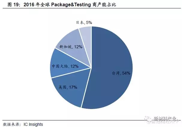 With the advantage of lower labor costs, China has a certain competitive strength in the labor-intensive IC packaging and testing industry, and it is also the most internationally competitive link in China's IC industry chain. At present, the domestic packaging and testing industry has a situation of foreign-owned, Sino-foreign joint ventures and domestic capital, and the domestic packaging industry has formed certain competitiveness. According to IC Insights data statistics, Changjiang Electronics, Huatian Technology, Tongfu Microelectronics and other domestic-funded enterprises have entered the top 20 global packaging and testing enterprises. As domestic companies continue to acquire or restructure overseas, domestic manufacturers are expected to further increase their market share in the future. Policy boost, semiconductor localization process accelerated In recent years, with the increasing supply and demand gap in China's semiconductor market, the state has also issued a series of policies to support the development of China's IC industry. From the perspective of investment, the national integrated circuit industry investment fund is now more focused on IC manufacturing; from the perspective of investment strategy, the fund focuses on the key enterprises in each industry chain; from the regional distribution, in Beijing, Shanghai, Wuhan, Fujian The investment in Jiangsu and Shenzhen accounts for 90% of the total investment. The establishment of large funds has greatly boosted the investment confidence of the industry and society in the IC industry. At present, local governments have also set up funds to support the integrated circuit industry. As of the first half of 2017, the scale of integrated circuit investment funds set up by local governments has exceeded 300 billion yuan. Driven by policies and funds, the semiconductor industry has begun to take shape: in the field of IC materials, China has broken through 12-inch silicon wafer technology and is expected to mass production by the end of this year. Advanced high-end targets, high-purity reagents, photoresists and other materials have been put on the market; in the field of IC equipment, domestic high-end lithography machines, etching machines and other equipment to achieve zero breakthrough, is gradually catching up with the international advanced level; In the field of IC design, domestic manufacturers represented by HiSilicon and Spreadtrum have begun to emerge, and their market share has gradually increased. In the field of IC manufacturing, the domestic market has broken through the 28nm process, and the 12-inch fab is also growing rapidly; in the field of IC packaging and testing. Domestic manufacturers already have certain competitive strength. Focusing on the target semiconductor is a highly capital-intensive and highly technology-intensive industry, and is a must for the world's major powers. GF Securities believes that China, as the world's largest consumer market for semiconductors, will enjoy the best growth opportunities in both the semiconductor industry and the national will, and the overall industry chain is expected to continue to benefit. It is recommended to focus on SMIC and Hua Hong Semiconductor, a foundry company with a certain scale, and ASM PACIFIC, a global semiconductor packaging and testing equipment manufacturer. SMIC: SMIC, a leading domestic foundry manufacturer, was established in 2000 and is the largest and the fourth largest wafer foundry in mainland China. At present, SMIC is the only IC manufacturer in the mainland to break through the 28nm process. The company currently offers foundry and technical services from 0.35 micron to 28nm. In 016, SMIC achieved sales revenue of US$2.914 billion. The company's gross profit margin remained at a high level, with a gross profit margin of 29.2% in 2016.
 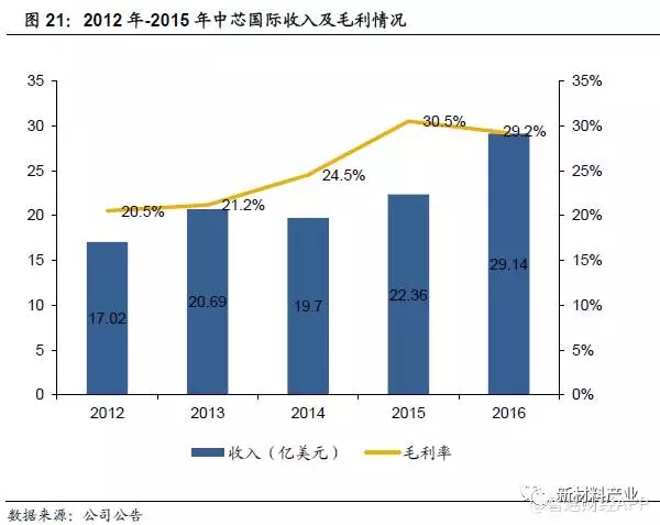 From the perspective of the composition of product revenue, the proportion of advanced processes below 65nm is on the rise. From the perspective of downstream products, the company's customers are mainly from the communications and consumer sectors, which account for more than 85% of revenue.
 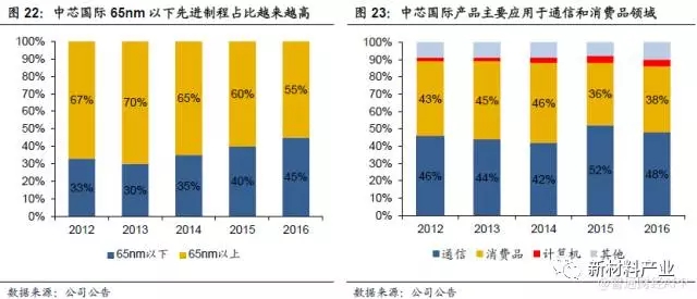 Hua Hong Semiconductor: Hua Hong Semiconductor Co., Ltd., the world's second largest 8-inch wafer foundry , focuses on the development and manufacturing of 200mm (8-inch) wafer semiconductors with technical applications ranging from 1.0μm to 90nm. According to IHS, Hua Hong Semiconductor is the world's second largest 200mm wafer foundry. As of June 2017, the company's 200mm wafer capacity reached 159,000 pieces per month. From the perspective of revenue scale and gross profit margin, the overall trend has been rising in the past five years. Among them, the company's revenue in 2016 reached 721 million US dollars, and the gross profit margin reached 30.5%.
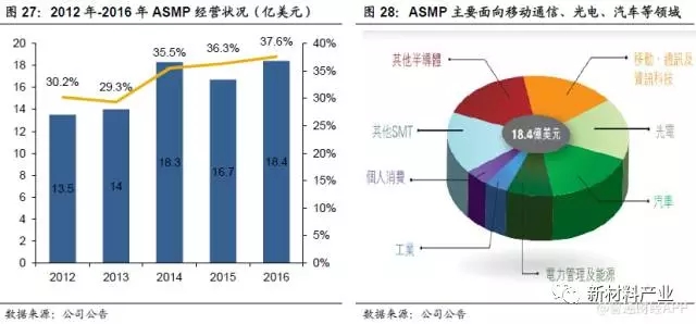
 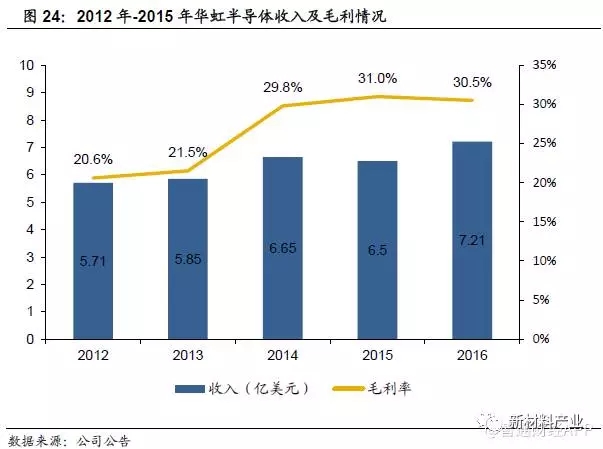 From the perspective of downstream applications, the company's products are mainly concentrated on embedded non-volatile memory and power devices, facing bank cards, bus cards, ID cards, IGBTs and other fields. ASM PACIFIC: ASM PACIFIC (ASMP), the world's largest supplier of semiconductor packaging equipment , was established in Hong Kong in 1975 and is the world's largest supplier of integration and packaging equipment for the semiconductor and LED industries. The company's equipment is mainly used in the microelectronics, semiconductor, optoelectronics and optoelectronics markets, including packaging and testing equipment such as solid crystal systems, wire bonding systems, epoxy systems, cutting ribs and forming systems. In 2016, the company's revenue reached US$1.84 billion and its gross profit margin was as high as 37.6%. The company's revenue is divided by region, with the largest proportion of revenue from China, reaching 54.6%. According to the business division, the post-process equipment (mainly packaging equipment) has the highest proportion of revenue, accounting for 50.6%; according to market application, mobile, communication and Information technology, optoelectronics and automobiles are the main sources of income for the company, accounting for about 50%.
  The main risk warning: the risk of the semiconductor industry's economic downturn again, the risk that the technical bottleneck cannot be broken in the process of semiconductor localization, the sales of the semiconductor downstream industry will not reach the expected risk, and the RMB will fluctuate greatly.
 Semiconductor products are mainly divided into four parts: integrated circuit (IC), optoelectronics, discrete devices and sensors. According to WSTS statistics, in 2016, IC sales accounted for 82%, optoelectronics accounted for 9%, discrete devices accounted for 6%, and sensors accounted for 3%. Since IC sales accounted for more than 80% of semiconductor sales for many years, IC is generally referred to as a semiconductor in the market. In addition, integrated circuits are differentiated according to different functional uses, mainly including four categories: microprocessor (about 18%), memory (about 23%), logic chip (about 27%), and analog chip (about 14%). At present, the global IC industry has two business models: IDM (Integrated Device Manufacturer) mode and vertical division mode.
  IDM refers to the business model that is completed by a company from design, manufacturing, packaging and testing to sales of its own IC products. Vertical division refers to the design, manufacture and packaging testing of ICs by professional IC designers (Fabless) and ICs. The business model undertaken by the manufacturer (Foundry) and the IC package tester (Package & Testing); At present, the IDM model still dominates the world. In 2016, global TOP20 manufacturers accounted for approximately 80% of global semiconductor sales. Among them, IDM manufacturers accounted for approximately 68% of the top 20, Fabless accounted for 18%, and Foundry accounted for 14%. The semiconductor industry is a cyclical industry, and its development has a high correlation with GDP, and the overall situation is positively correlated. In recent years, with the development of next-generation information technology in the fields of artificial intelligence, big data, Internet of Things, AR/VR, and wearable devices, the semiconductor industry has re-entered a new round of business cycle.
  According to the statistics of WSTS, the world's semiconductor trade statistics organization, the global semiconductor sales growth rate was 5.21% from 2003 to 2016, of which global semiconductor sales in 2016 reached 338.9 billion US dollars, an increase of 1.12%. WSTS expects global semiconductor sales to reach US$396.6 billion in 2017, a year-on-year growth rate of 17%. By 2020, the entire market is expected to reach a market size of US$400 billion.
  In recent years, the demand for China's semiconductor market is strong, and the growth rate of the IC market is significantly higher than the global growth rate. According to WSTS statistics, China's semiconductor consumption in 2016 was 107.5 billion US dollars, accounting for 32% of the global total. It has surpassed the United States, Europe and Japan to become the world's largest market. At the same time, according to the China Semiconductor Industry Association (CSIA) statistics, China's IC sales in recent years maintained a double-digit growth rate, of which China's IC sales in 2016 increased by 20.1% year-on-year.
  But on the whole, the self-sufficiency rate of the domestic IC market is still at a low level, and the products are mainly imported from abroad.
  IC materials: domestic manufacturers step into the development of fast lane IC materials are mainly divided into IC manufacturing materials and IC packaging materials. The IC manufacturing materials mainly include silicon wafers and substrates, photomasks, photoresists, electronic gases, CMP materials, targets, etc.; IC packaging materials include laminated substrates, lead frames, bonding wires, molding compounds, and bottoms. Filler, liquid sealant, die bonding material, solder ball, etc. According to the International Semiconductor Industry Association (SEMI) report, the global IC manufacturing materials market was $24.7 billion in 2016 and the packaging materials market was $19.6 billion. Among them, among silicon manufacturing materials, silicon wafers account for the highest proportion of 32%, and silicon wafers and masks, electronic gases, CMP materials, and photoresists account for nearly 80% of the total, which is affecting the IC manufacturing process. The most important material. The wafer is the substrate for IC processing. From the development history of the wafer material, it can be roughly divided into three generations: the first generation is represented by germanium and silicon; the second generation is mainly gallium arsenide and indium phosphide; The third generation is gallium nitride, silicon carbide, and the like. At present, most wafers still use silicon as the main raw material. Judging from the global competition in silicon wafer materials, this market is dominated by Japanese manufacturers. According to the 2015 SEMI statistics, Japan's Shin-Etsu and SUMCO are leading manufacturers in the wafer production industry, and the two companies together account for about 50% of the market. According to the SEMI report, the size of the IC manufacturing materials market in China in 2016 was US$6.53 billion, which has become the fourth largest IC manufacturing materials market in the world, second only to Taiwan, South Korea and Japan. IC equipment: The trend of localization began to show that IC equipment is the upstream supporting equipment for IC production, and IC equipment is basically needed in IC design, manufacturing, packaging and testing. According to different functional uses, IC devices are generally classified into three categories: IC manufacturing equipment, IC packaging equipment, and IC testing equipment. Among them, IC manufacturing equipment has the largest variety and the largest proportion, such as lithography machine, etching equipment, film deposition and other core wafer processing equipment; IC packaging equipment mainly has bonding machine, laminating machine, etc.; IC test equipment mainly includes sorting machine , test machine, probe station, etc., suitable for the end of the IC design, manufacturing, packaging test.
  The IC equipment industry has high technical barriers, and currently European, American and Japanese manufacturers still occupy an absolute dominant position. Applied Materials, ASML, Tokyo Electronics, and Lam Research are the world's top four semiconductor device manufacturers with market shares of approximately 19%, 18%, 16%, and 15%, respectively. The rapid development of domestic downstream IC production links has driven the strong demand for domestic IC equipment market. According to SEMI's survey, China's semiconductor equipment market in 2016 was US$6.66 billion, up 31.8% year-on-year, and the fastest growth rate in the world, becoming the third largest semiconductor equipment market after Taiwan and South Korea. According to SEMI estimates, the demand for IC equipment by Chinese local companies will increase rapidly between 2018 and 2020. The estimated investment in IC equipment is US$10.8 billion, US$11 billion and US$17.2 billion, respectively. With the continuous improvement of market demand, domestic IC equipment manufacturers continue to increase research and development efforts. In the past two years, China has made breakthroughs in many key equipment fields. IC design: The domestic manufacturer's emerging IC design, Integrated Circuit Design, is the process of transforming the system, logic and performance design requirements into a specific physical layout. The IC design flow is divided into several steps: specification customization, hardware language description, simulation and simulation verification, logic synthesis, circuit simulation verification, circuit layout and surround, circuit detection, and mask production. According to IC Insights data, in the field of pure IC design (Fabless), the United States has the largest market share. In 2016, the total capacity of IC Fabless in the United States accounted for 62% of the global total. Qualcomm and Broadcom are leading companies in the IC Fabless industry, with combined revenues accounting for 51% of the top 10 revenues. Among them, Qualcomm's revenue in 2016 was 15.4 billion US dollars, and Broadcom's revenue was 15.3 billion US dollars.
  Benefiting from the demand in the domestic downstream mobile, communications and other fields, the competitiveness of domestic IC designers began to emerge. According to IC Insights statistics, there were only one mainland Chinese company in the TOP50 Fabless business in 2009. By 2016, the number of mainland Chinese enterprises has reached 11 and the combined market share has increased to 10%. Among them, Huawei HiSilicon and Spreadtrum have become among the top 10 Fabless in the world.
  IC manufacturing: The policy support is the strongest, and domestic manufacturers are eager to catch up with IC manufacturing to complete the process of integrated circuit etching on the wafer. The IC manufacturing process includes surface grinding, cleaning, coating, multiple lithography, ion implantation, etching, heat treatment, decanting, polishing, cleaning, inspection, packaging and other processes. At present, international leading manufacturers have developed process technology to 10nm level. Leading manufacturers such as TSMC and Samsung have achieved mass production in 10nm process. Intel and Grofund expect to achieve mass production by the end of this year. In addition, TSMC is taking the lead in developing 7nm process technology.
  According to IC Insights data, Taiwan has the largest market share in the field of pure IC manufacturing (Foundry). In 2016, the total production capacity of Foundry in Taiwan accounted for 73% of the global total. Among them, TSMC's revenue was US$28.57 billion, accounting for 58% of the global market share.
  IC manufacturing is a capital- and technology-intensive industry and is the focus of national policies and funds. Among the funds invested in IC manufacturing, 12-inch fabs accounted for the largest proportion. Mainly because the current global demand for 12-inch wafers is the largest, while the domestic production capacity is very low. According to China's electronic network statistics, the current global demand for 12-inch semiconductor silicon wafers is about 5.1 million units. The total monthly capacity of the 12-inch factory in mainland China is only about 460,000 pieces. The huge capital injection has driven the rapid growth of the domestic 12-inch wafer production line. According to estimates by the International Semiconductor Association (SEMI), between 2017 and 2020, 62 new fabs will be put into production worldwide, and 26 of them will be located in mainland China, accounting for 42% of the global total. Most of the new 26 fabs are 12-inch fabs. At present, the 12-inch wafer fab has a production capacity of about 630,000 pieces. In the future, the 12-inch capacity of the mainland will reach 1.09 million units per month. The rapid expansion of domestic manufacturers' production capacity has also led to a rapid increase in their sales scale. As a leading enterprise in the domestic IC manufacturing industry, SMIC and Huahong Semiconductor have taken advantage of the trend. In recent years, the market share has increased year by year. At present, both companies are among the top ten founders in the world. IC packaging test: domestic manufacturers have certain competitive strength. IC packaging and testing is a labor-intensive industry, and the overall barriers to entry are not high. In terms of regional distribution, it is mainly concentrated in the Asia-Pacific region. According to IC Insights statistics, ASE, Amkor, Changjiang Electronics, and çŸ½å“ are the top four packaging and testing companies in the world.
  With the advantage of lower labor costs, China has a certain competitive strength in the labor-intensive IC packaging and testing industry, and it is also the most internationally competitive link in China's IC industry chain. At present, the domestic packaging and testing industry has a situation of foreign-owned, Sino-foreign joint ventures and domestic capital, and the domestic packaging industry has formed certain competitiveness. According to IC Insights data statistics, Changjiang Electronics, Huatian Technology, Tongfu Microelectronics and other domestic-funded enterprises have entered the top 20 global packaging and testing enterprises. As domestic companies continue to acquire or restructure overseas, domestic manufacturers are expected to further increase their market share in the future. Policy boost, semiconductor localization process accelerated In recent years, with the increasing supply and demand gap in China's semiconductor market, the state has also issued a series of policies to support the development of China's IC industry. From the perspective of investment, the national integrated circuit industry investment fund is now more focused on IC manufacturing; from the perspective of investment strategy, the fund focuses on the key enterprises in each industry chain; from the regional distribution, in Beijing, Shanghai, Wuhan, Fujian The investment in Jiangsu and Shenzhen accounts for 90% of the total investment. The establishment of large funds has greatly boosted the investment confidence of the industry and society in the IC industry. At present, local governments have also set up funds to support the integrated circuit industry. As of the first half of 2017, the scale of integrated circuit investment funds set up by local governments has exceeded 300 billion yuan. Driven by policies and funds, the semiconductor industry has begun to take shape: in the field of IC materials, China has broken through 12-inch silicon wafer technology and is expected to mass production by the end of this year. Advanced high-end targets, high-purity reagents, photoresists and other materials have been put on the market; in the field of IC equipment, domestic high-end lithography machines, etching machines and other equipment to achieve zero breakthrough, is gradually catching up with the international advanced level; In the field of IC design, domestic manufacturers represented by HiSilicon and Spreadtrum have begun to emerge, and their market share has gradually increased. In the field of IC manufacturing, the domestic market has broken through the 28nm process, and the 12-inch fab is also growing rapidly; in the field of IC packaging and testing. Domestic manufacturers already have certain competitive strength. Focusing on the target semiconductor is a highly capital-intensive and highly technology-intensive industry, and is a must for the world's major powers. GF Securities believes that China, as the world's largest consumer market for semiconductors, will enjoy the best growth opportunities in both the semiconductor industry and the national will, and the overall industry chain is expected to continue to benefit. It is recommended to focus on SMIC and Hua Hong Semiconductor, a foundry company with a certain scale, and ASM PACIFIC, a global semiconductor packaging and testing equipment manufacturer. SMIC: SMIC, a leading domestic foundry manufacturer, was established in 2000 and is the largest and the fourth largest wafer foundry in mainland China. At present, SMIC is the only IC manufacturer in the mainland to break through the 28nm process. The company currently offers foundry and technical services from 0.35 micron to 28nm. In 016, SMIC achieved sales revenue of US$2.914 billion. The company's gross profit margin remained at a high level, with a gross profit margin of 29.2% in 2016.
  From the perspective of the composition of product revenue, the proportion of advanced processes below 65nm is on the rise. From the perspective of downstream products, the company's customers are mainly from the communications and consumer sectors, which account for more than 85% of revenue.
  Hua Hong Semiconductor: Hua Hong Semiconductor Co., Ltd., the world's second largest 8-inch wafer foundry , focuses on the development and manufacturing of 200mm (8-inch) wafer semiconductors with technical applications ranging from 1.0μm to 90nm. According to IHS, Hua Hong Semiconductor is the world's second largest 200mm wafer foundry. As of June 2017, the company's 200mm wafer capacity reached 159,000 pieces per month. From the perspective of revenue scale and gross profit margin, the overall trend has been rising in the past five years. Among them, the company's revenue in 2016 reached 721 million US dollars, and the gross profit margin reached 30.5%.
  From the perspective of downstream applications, the company's products are mainly concentrated on embedded non-volatile memory and power devices, facing bank cards, bus cards, ID cards, IGBTs and other fields. ASM PACIFIC: ASM PACIFIC (ASMP), the world's largest supplier of semiconductor packaging equipment , was established in Hong Kong in 1975 and is the world's largest supplier of integration and packaging equipment for the semiconductor and LED industries. The company's equipment is mainly used in the microelectronics, semiconductor, optoelectronics and optoelectronics markets, including packaging and testing equipment such as solid crystal systems, wire bonding systems, epoxy systems, cutting ribs and forming systems. In 2016, the company's revenue reached US$1.84 billion and its gross profit margin was as high as 37.6%. The company's revenue is divided by region, with the largest proportion of revenue from China, reaching 54.6%. According to the business division, the post-process equipment (mainly packaging equipment) has the highest proportion of revenue, accounting for 50.6%; according to market application, mobile, communication and Information technology, optoelectronics and automobiles are the main sources of income for the company, accounting for about 50%.
  The main risk warning: the risk of the semiconductor industry's economic downturn again, the risk that the technical bottleneck cannot be broken in the process of semiconductor localization, the sales of the semiconductor downstream industry will not reach the expected risk, and the RMB will fluctuate greatly.
RXIRY Low Light-level Night Vision Gunsight

gunsinghts, night vision, infared,6X magnification
Rxiry (Jiangsu) Optoelectronic Co., Ltd , https://www.rxiryrangefinder.com